Syskey
Syskey Technology Co., Ltd.
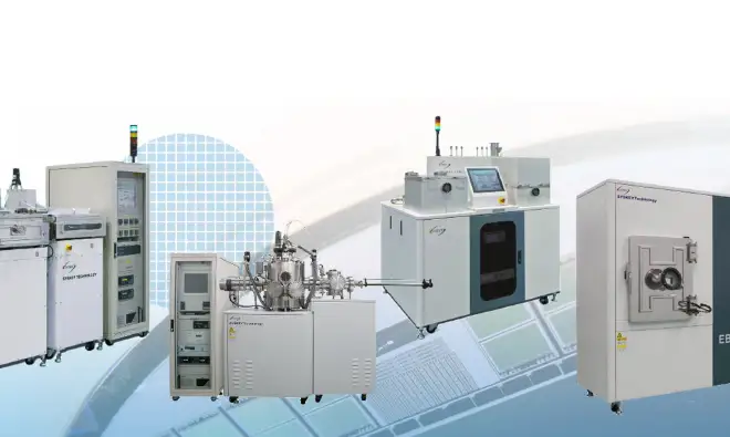
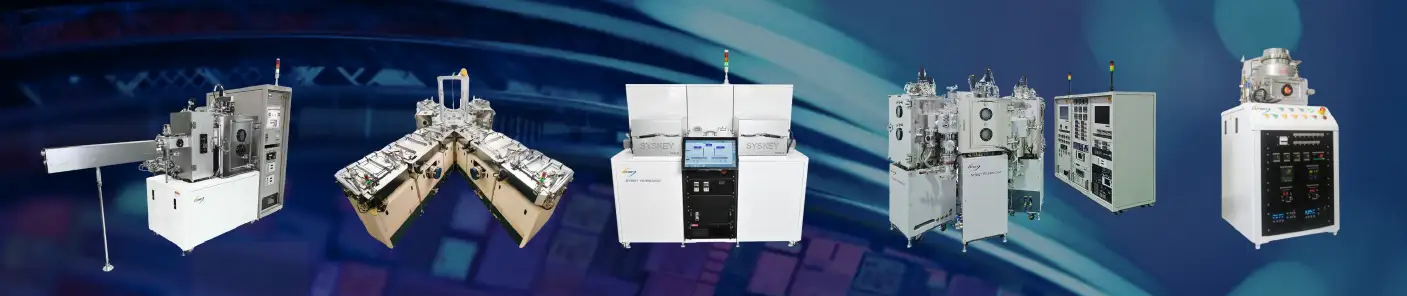
As your dedicated thin film device partner, Syskey Technology provides you with comprehensive semiconductor deposition solutions, including PVD, CVD, ALD and plasma etching. These systems are available in manual, semi-automated or fully automated configurations.
With the rapid evolution of the semiconductor industry, Syskey is continuously developing and renewing its thin film technologies. Syskey also specializes in customization to meet your specific requirements, whether for R&D applications or industrial production.

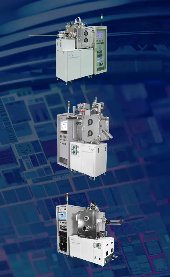
PVD
The physical vapor deposition (PVD) system enables deposition through a
phase change from solid to gaseous state of the material, without any
chemical reactions. The evaporation of the material can be achieved using
different methods, such as sputtering, thermal, or electron beam.
Application: semiconductors, solar cells, optical devices and so on.
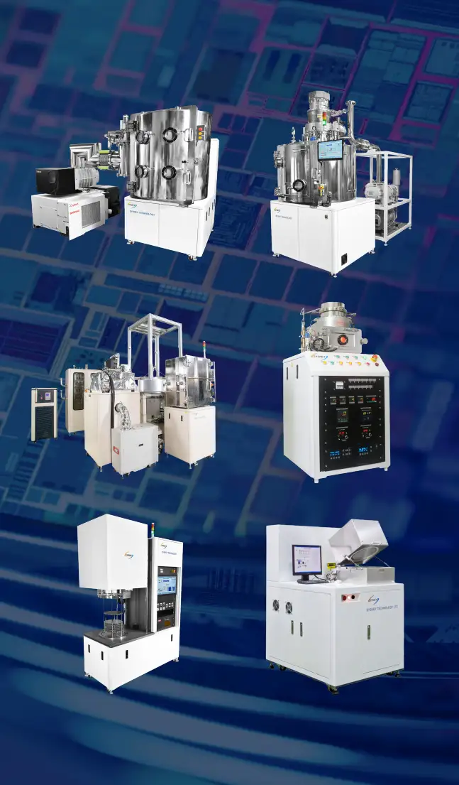
Magnetron Sputter
The thin film is deposited by sputtering the material from the target, which is bombarded by argon or nitrogen plasma. It offers both DC and RF power options according to the conductivity of the targrets.
Related products: Co-sputter /UHV Sputter / Muti-layer Sputter / In-Line Sputter.
Thermal Evaporation
A simple resistive heating method for evaporating directly the material onto the substrate. It can control multiple heat sources simultaneously for both electrode deposition and depositing single-layer materials. The deposition rate is faster than sputtering.
Related products: Metal Thermal / Organic Material.
Electron Beam Evaporation
The evaporation of the material is achieved by the electron beam generated by a tungsten filament. This method can melt materials at higher temperatures, e.g. for tungsten and graphite, and offers better control over the evaporation rate compared to thermal evaporation.
Related products: UHV E-Beam / Lift off.
CVD
Chemical vapor deposition (CVD) facilitates the formation of high-quality thin films by exposing substrates to volatile precursors that react and decompose on surfaces.
PECVD: (Plasma Enhanced Chemical Vapor Deposition) Plasma-enhanced technology allows depositing thin films at lower temperatures (less than 350°C) without losing film quality. It provides exceptional uniformity, good step coverage, and high packing density for semiconductors, display, and optical applications. It is also used more widely in the semiconductor industry than other CVD systems.
LPCVD: (Low Pressure Chemical Vapor Deposition) Heat-initiated precursor reaction system with low pressure to reduce the gas phase reactions and promote uniformity across substrates. Enables batch processing with improved thickness uniformity (< ±3%) and reduced production costs, ideal for CNT, graphene, and high-temperature processes up to 1700°C.
ICP-CVD: (Inductively Coupled Plasma CVD) Advanced ICP plasma source provides higher plasma concentration, lower energy loss, and superior reaction rates compared to PECVD. It enables various film depositions at lower temperatures while maintaining film quality for 2D materials and advanced applications.
FPD-PECVD: (Flat Panel Display PECVD) Large-scale system designed for LCD panel manufacturing, processing amorphous silicon (a-Si), silicon oxide (SiOx), silicon nitride (SiNx), and multi-layer depositions on glass substrates up to 550 x 650 mm² with exceptional uniformity.
Diamond Like Carbon: (DLC) Specialized coating system producing amorphous nano-composite carbon materials with diamond-like properties including high hardness, corrosion resistance, and low friction. It can be utilized for semiconductor molds, tool coatings, medical instruments, and optical applications requiring superior wear resistance.
Batch Type PECVD: High-throughput batch processing system specifically designed for parylene deposition. The substrate can both rotate and orbit. This solution can also be applied to electrooptical packaging and PCB insulation.
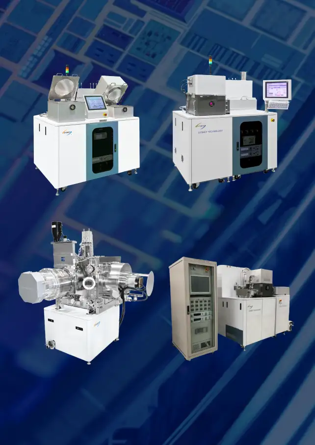
ALD
Atomic layer deposition (ALD) systems utilize sequential gas-phase chemical processes to deposit thin films with atomic-scale precision, excellent uniformity, and superior conformality, even on complex substrate geometries. Applications: high-k gate oxides, solar cells, OLEDs, MEMS, optical functional films and encapsulation.
Thermal ALD: Sequential self-limiting and continuous reaction of precursors with heated substrate surfaces at temperatures typically ranging from 150 to 350°C. It delivers excellent thin-film uniformity (less
than ±1%) with high conformity for complex geometries.
PEALD: (Plasma-enhanced ALD) Advanced plasma-enhanced system using plasma energy to crack precursor materials instead of only thermal energy from the heated substrate. This enables low-temperature processing while maintaining atomic-scale control for temperature-sensitive substrates. The uniformity of the achieved thin films is also less than ±1%.
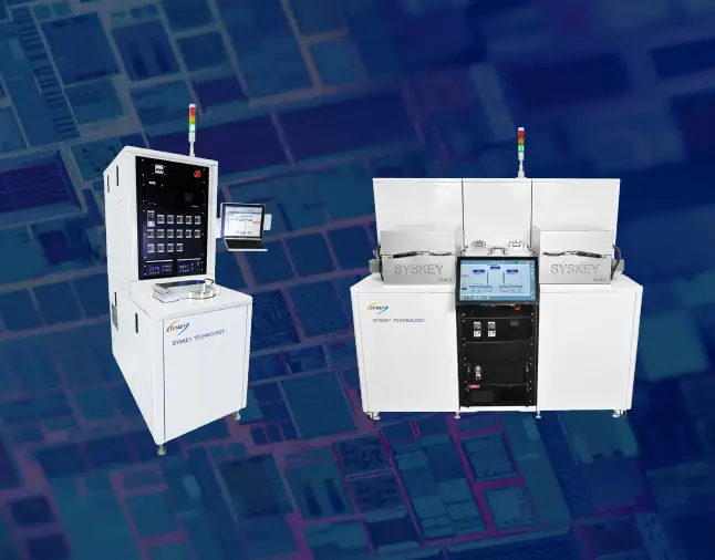
Dry etching
Dry etching, also known as plasma dry etching, is a technique that removes materials from the surface using reactive ions. This process enables highly directional (anisotropic) etching, allowing the generation of high aspect ratio structures, such as deep holes and capacitor trenches. These structures have a variety of applications in semiconductor and PCB fabrication.
RIE: (Reactive Ion Etching) A chemical-physical process in semiconductor fabrication, offering precise control over etching profile, rate, uniformity, and repeatability. It enables both isotropic and anisotropic etching. This system can control gas and plasma, enabling the high-quality thin film etching.
ICP-RIE: (Inductively Coupled Plasma RIE) An advanced form of RIE, enhanced by the addition of a high-density plasma source. The highdensity plasma and low-pressure result in very high etch rates, with a more anisotropic profile. This system ensures accurate gas and plasma control for high-precision thin film etching.
Ion Beam Etching: An advanced physical etching technique that uses a high-energy focused ion beam (typically argon ions) to remove material from a substrate with exceptional uniformity and control. It can be applied to a wide range of materials, including metals, oxides, semiconductors, and organic compounds.
ALE: (Atomic layer etching) A highly precise etching technique that can control material removal at the atomic level. Plasma-based ALE operates through cyclic gas exposure and ion bombardment, which allows layer-bylayer removal with very low damage, enabling the creation of very small and complex features.
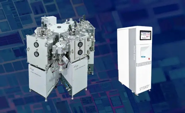
Cluster & Mini Line
Cluster Tool: Multi-chamber system which can integrate sputtering, etching, PECVD, evaporator, ALD, annealing, plasma cleaning and cooling down system within one platform according to your requirements. It features robotic substrate transfer, and flexible configurations for semiconductors, solar cells, LED, OLED, OPV, and FPD applications.
Mini Line: This series of smaller systems are developed for faster experiments and limited spaces. It is designed for 2-inch substrates and is compatible with thermal, sputter, PECVD, PEALD, RIE, ICP-RIE, and E beam systems. With precise gas control and real-time monitoring, it delivers excellent uniformity (±3% for thermal and sputter, and ±1% for PEALD). Ideal for R&D and small-scale production.
![]()
![]()
Searching for a partner with whom you can develop your projects and meet demanding industry requirements
Linkedin Syskey Europe, powered by Euris Semiconductor
![]()
![]()