FRT
FRT GmbH, a FORMFACTOR company
THE ART OF METROLOGY
FRT offers a comprehensive range of metrological surface measuring systems for the non-destructive investigation of topography, profile, film thickness, roughness, abrasion and many other properties. More than 500 reputable international companies from the automotive, semiconductor, MEMS, optical, photovoltaic and many other industries equip their R&D and production departments with FRT metrology systems.
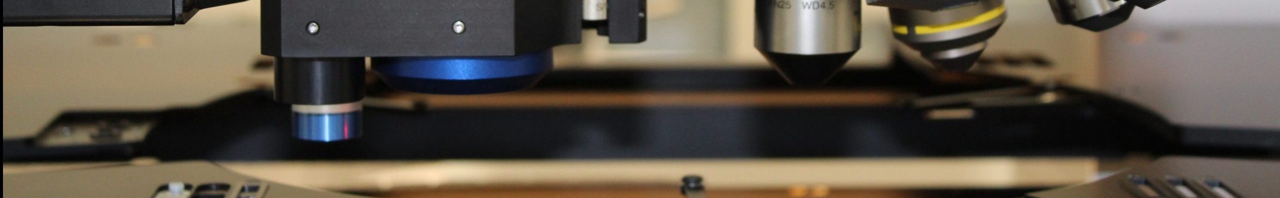
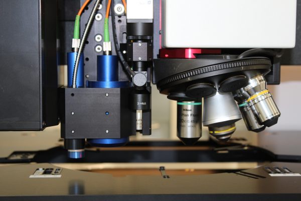
Multi-sensor technology
Our Technologies: point, line and field of view sensors, optionally atomic force microscopy
The FRT Multi-Sensor Technology offers you the possibility to combine different measuring principles in one single tool and thus allows maximum flexibility.
For the measurement of topography, roughness, sample thickness, layer thickness and many other surface parameters, the FRT surface measuring systems can be equipped with various sensors. FRT offers a wide range of point, area and film thickness sensors which are fully integrated into the tool and can be flexibly arranged and combined. The possibility of retrofitting sensors opens up further options for flexible adaptation to future measuring tasks, such as individual and exchangeable sample holders.
Wafer Metrology
The standard fully automated wafer metrology tools – FE, FS, AP and DI
The standard fully automated wafer metrology tools – FE, FS, AP and DI – combine the capabilities of the worldwide established MicroProf ® 300, with a wafer handling system within an Equipment Front End Module (EFEM). With fully SEMI-compliant metrology solutions and almost maintenance-free hardware components, the MicroProf ® with EFEM is configurable for any front end high-volume fab (FE), for a wide range of applications in the silicon wafer foundry (FS), applications at different 3D packaging process steps (AP) or comprehensive inspection applications (DI).
Download data sheet:
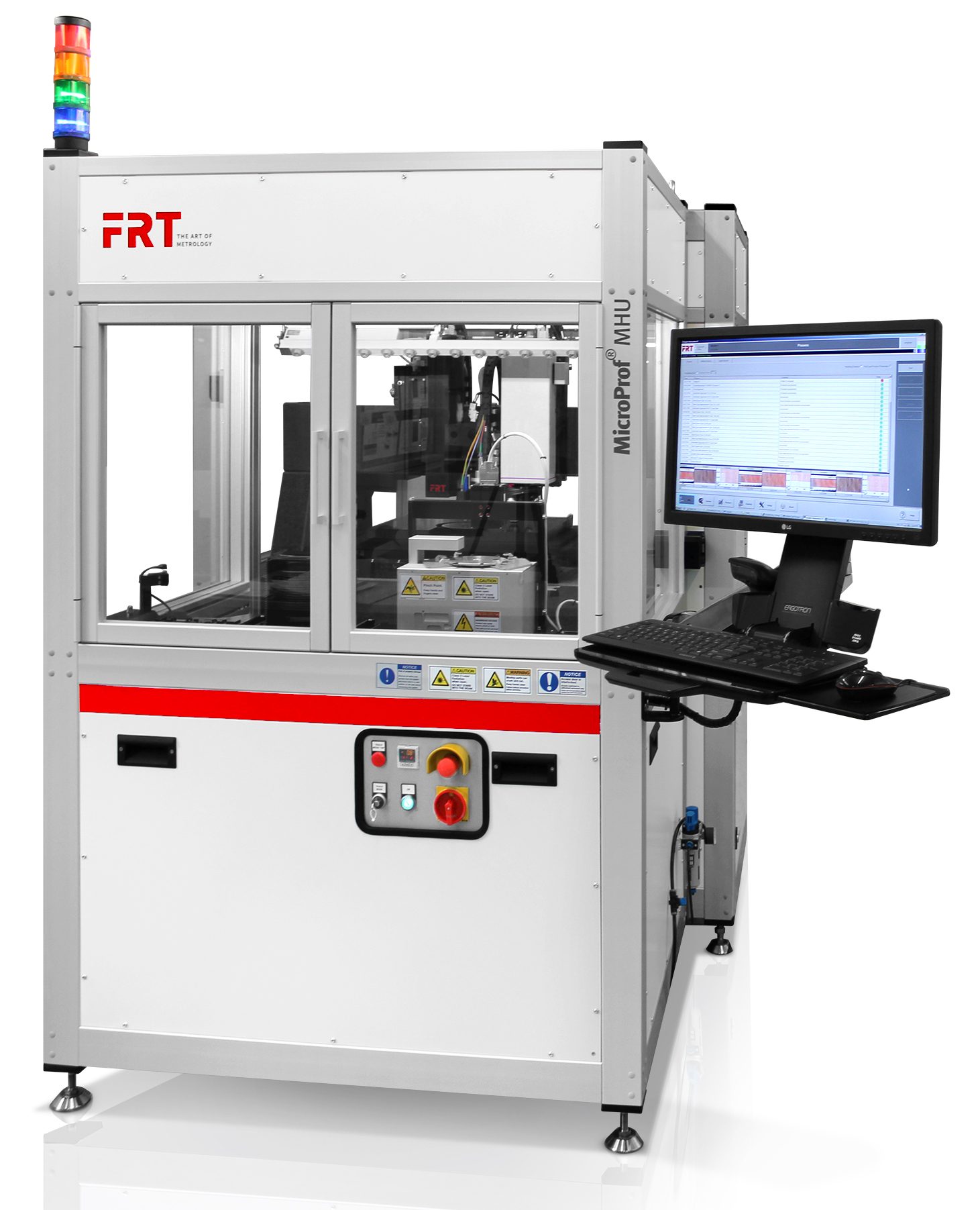
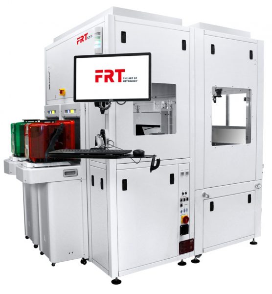
Metrology Tool MicroProf ® MHU with Material Handling Unit
The MicroProf ® MHU is a metrology tool with material handling unit, which was developed especially for the semiconductor, MEMS, sapphire and LED industry. Typical applications are the measurement of bare and coated wafers or structured wafers in various lithographic process steps.
Due to a robotic arm with two vacuum end effectors, the device has a very high throughput of up to 220 wafers per hour. It is able to process wafer sizes from 2 to 8 inches. Up to 4 open cassettes can be processed and it is possible to integrate a pre-aligner and an OCR reader in the device.
Download data sheet: