
Arradiance
Arradiance Atomic Layer Deposition
Molecular InnovationTM – Enabling Technologies for Our World and Beyond.
Systems for Atomic Layer Deposition, Foundry of Nanofilms and Technology Services in the field of ALD and Nanofilm. Supported markets are Energy storage, Medical devices, Solar PV, High Energy Physics, Semiconductor Research, Catalyst Research, Superconductors.
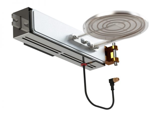
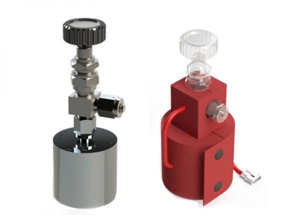
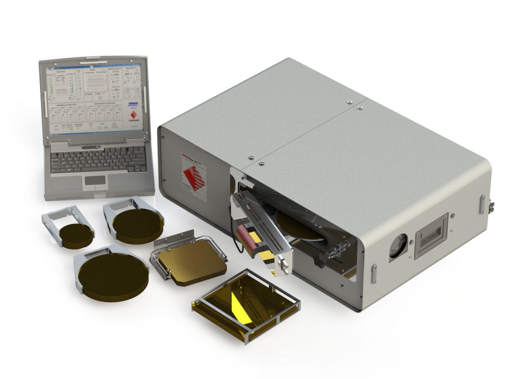 Thermal ALD system, GEMStar XT
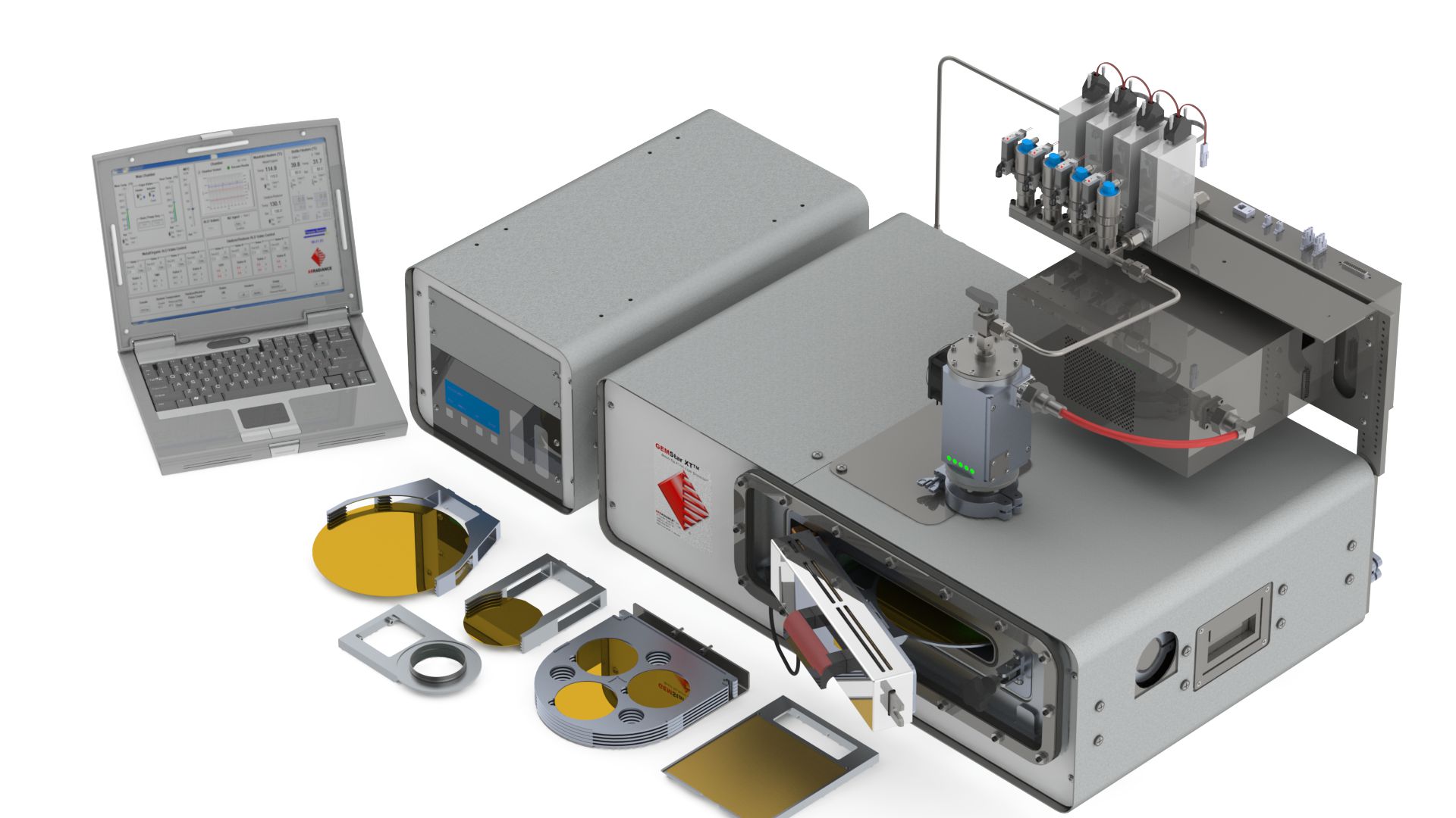
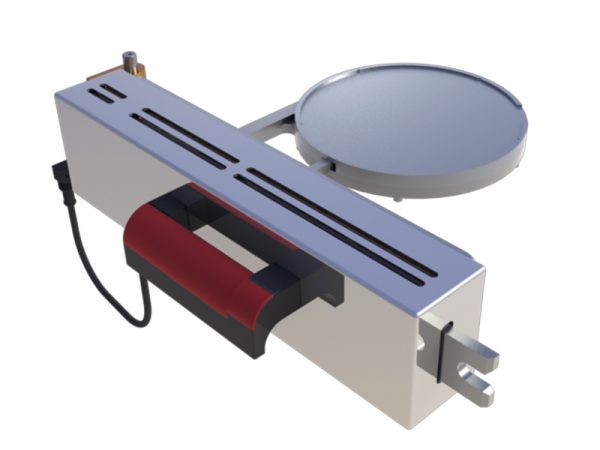
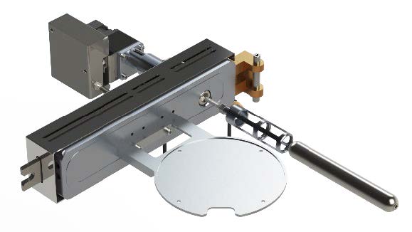
PEALD System, GEMStar XT-xP
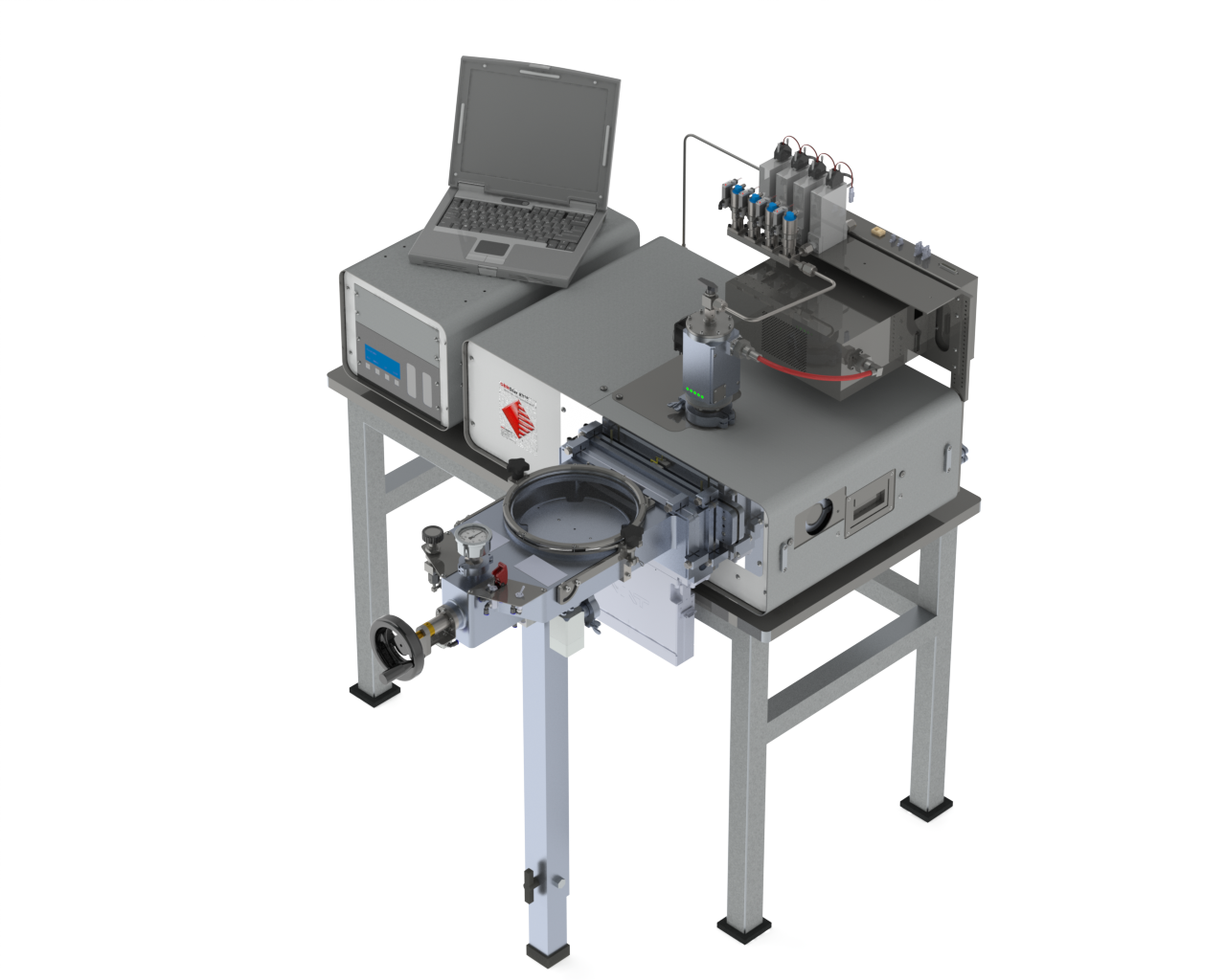
The Arradiance GEMStar product family provides high-quality ALD equipment in a compact benchtop platform. We offer systems with one manifold including four precursor lines for pure thermal ALD, up to PEALD (Plasma Enhance Atomic Layer Deposition) systems with two manifolds, including eight precursors and up to 4 plasma gases.
To meet any budget, we offer cost-effective thermal ALD systems with the ability to be upgraded to high-end PEALD systems. A Pulsed Vapor Push, suitable for low vapor pressure materials, is included in each system.
The GEMFlow software enables easy programming for complicated nanolaminate films and stores the history of all process and system parameters.
- Data Sheet GEMStarXT (PDF)
- Data Sheet GEMStarXT-R (PDF)
- Data Sheet GEMStarXT-P (PDF)
Options
- Interface for Glovebox
- LoadLock
- Extra Precursor Bottle
- Extra Material Heater Jackets
- 500ºC heated substrate plates
- Ebara Dry Pump
- Kit for Ozone generation and abatement
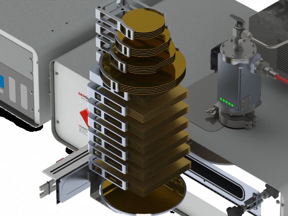
- Carrier for batch processing
- Particle coating, with rotational particle canister
- QCM (Quartz Crystal Monitor).
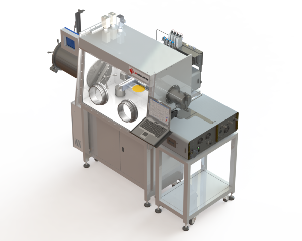
GEMStar XT-R and GEMStar-XT-P integrated with Glovebox
Glove Box Integration of GEMStar-XT-R and GEMStar-XT-P – Arradiance
Both, the GEMStar-XT-R and the GEMStar-XT-P are connected to a glovebox. The GEMStar is outside the Glovebox which has many advantages, for instance:
- more space in the glove box
- the system is easier to maintain
- uncomplicated precursor bottle exchange or refill
- the sensitive glovebox atmosphere will be much less influenced by the thermal massData Sheet GEMStar XT and XT-P GB Glovebox Interface (PDF)
Data Sheet GEMStar XT MULTI-TRAP System (PDF)
Heated Platen Option for Arradiance GEM Star XT HP TM
This platen option was developed to enable our GEMStar System to reach higher process temperatures.
With these plates, the substrate temperature can be increased to 450° C.
Data Sheet GEMStar XT HP (PDF)
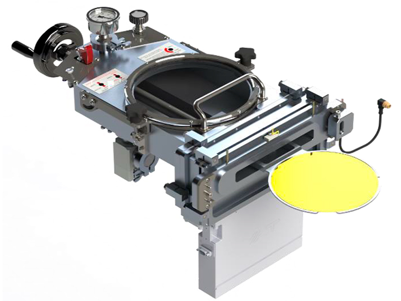
Load Lock Option for Arradiance GEM Star XT LL TM
This Load Lock System is optimized to use
with the GEMStar XT Benchtop ALD Systems.
It enables the control of atmospheric exposure
of the process reactor and substrate
during exchange.
Data Sheet GEMStar XT-LL (PDF)
Substrate holders for Arradiance GEM Star XT LL TM
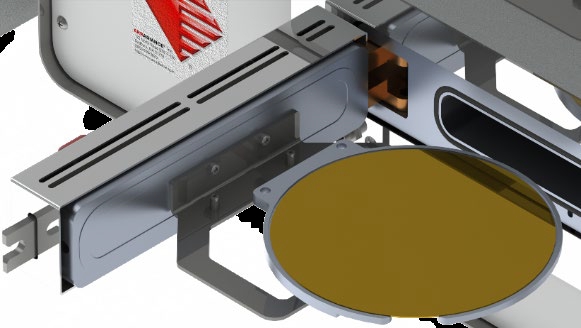
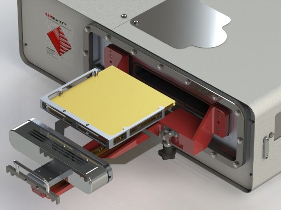
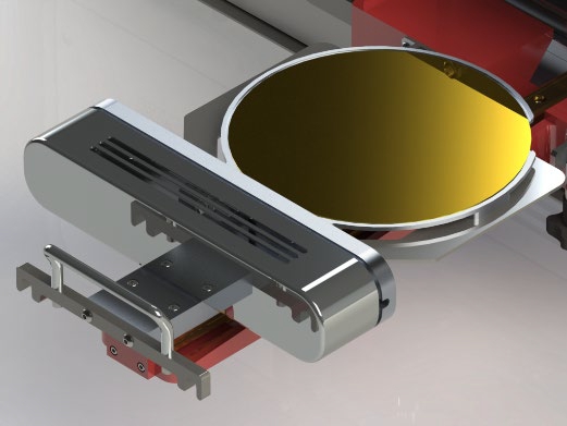
To achieve maximum user flexibility, Arradiance has engineered a door mounted End Effector system option that allows “Tool less” change of substrate end effector holders and cassettes allowing the GEMStar XT system to process a wide range of standard substrates from Si wafers to Solar Cells.
Front loading tray system for GEMStar XT-LL
Enabling thermal ALD processing of large substrates up to M12 Solar Panels, Arradiance has engineered a front-loading tray system. This system allows tool-less exchanges of Single Substrate End Effectors and Cassettes ranging from 100 mm Diameter to Solar M12 (210 mm Square) substrates
Particle Coating Door Option for GEM Star XT-LL
This option is designed for offering the GEMStar Benchtop ALD System the possibility to simultaneously coat particles and wafers both, on a desktop or in connection with a glovebox.
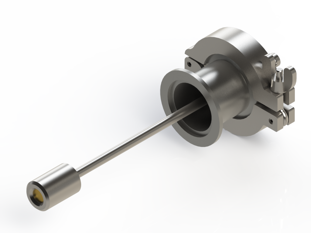
The NW-25 ALD Vacuum Gauge Protector utilizing our patent pending TPGP technology
Included with new systems and available as a spare/upgrade
This QCM (Quartz Crystal Microbalance) mounts directly to the standard KF-40 Metrology Port.
It enables in-situ monitoring of film growth and other surface studies like desorption/absorption.
Datasheet QCM (PDF)
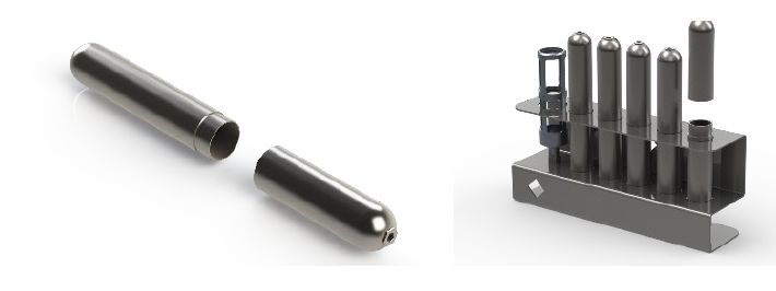
 Precursor bottle and heater jacket
Arradiance Precursor Bottle and Heater Jacket

Do You Have Questions?
Feel free to send us an email:
loeffen@euris-semiconductor.com
Ward Loeffen

Do You Have Questions?
Feel free to send us an email:
sage@euris-semiconductor.com
+33 476 35 0707
Stéphane Sage
ALD – Atomic Layer Deposition
What is Atomic Layer Deposition (ALD)?
Atomic layer deposition (ALD)
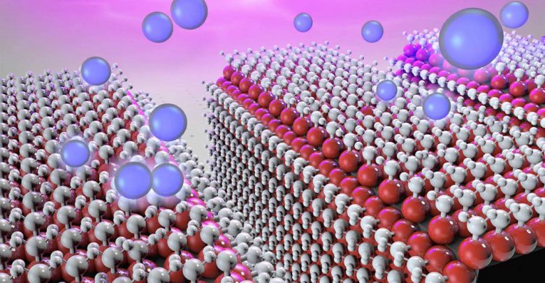
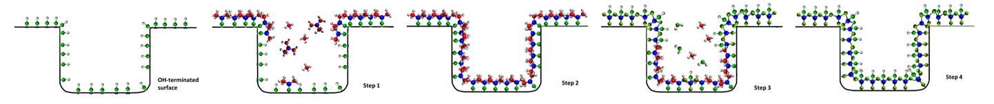
is a thin film deposition method using a stepwise application of a chemical process in the gas phase. The method is based on chemical vapour deposition. Most ALD reactions utilize two chemicals called precursors (or „reactants“). These precursors react with the surface of a substrate-material one at a time in a step by step, self-limiting process. By repeating exposure to separate precursors, a thin film will slowly grow. The main application of ALD is in micro-and nanoelectronics int terms of step coverage and thickness uniformity. Further, strongly growing applications are in the fields of photovoltaic, energy storage, and catalyst.
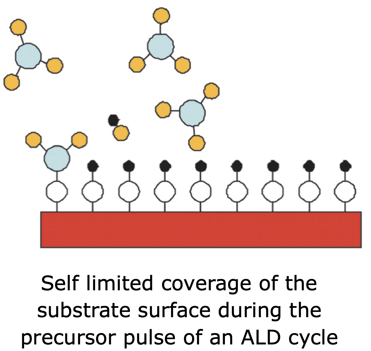
ALD Cycle, based on Cremers et al., 2019
What are typical applications for ALD?
- High-k materials, for instance HfO2 and other oxides
The excellent thickness control of ALD is perfect for this application. - Ideal for structures with High Aspect Ratio, (>100:1)
- Nanolaminates / Superlattices
- As passivation layer in PV Cells, development of PV cells
- Multilayer systems, for instance materials based on perovskite
- Particle coating
- Coating of porous materials.
Advantages of ALD:
- Layer thickness of a few Nanometer with thickness control <1nm.
- Best uniformity on large area substrates
- Precise control of Stoichiometry
What is Thermal ALD:
Thermal ALD is a deposition process at relatively high temperatures ranging from 150oC to 450oC. It provides high control of thickness, independently of substrate geometry and reactor design.
What is Plasma ALD or PEALD (Plasma Enhanced Atomic Layer Deposition):
Plasma activates the precursors‘ reactivity, allowing the deposition temperature to be lowered without affecting the quality of the film. More precursors can be used, allowing more materials to be deposited and thus more materials to be coated.
Why Atomic Layer Deposition:
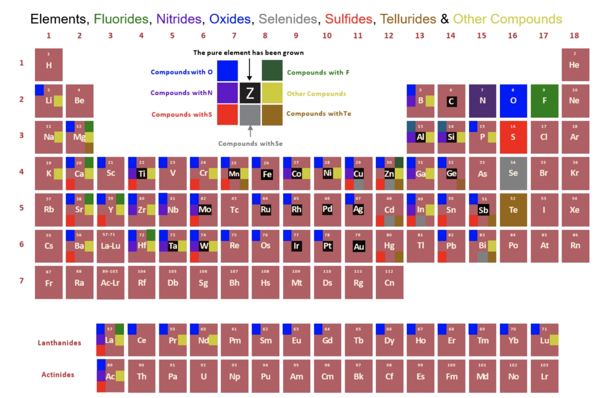
The inherent strength of ALD technology is its ability to utilize most of the substances available in the periodic table, as shown below.
Furthermore, conformality and the ability to adapt to various substrates, shapes, and high aspect ratio structures producing uniform, pinhole-free single material and nano-laminate coatings, has created broad interest in many fields.
Euris Supplier Arradiance process and equipment technologies were forged in the most challenging ALD Nanofilm environment: electrically functional nanofilms on substrates possessing both high surface areas (>9m2) and high aspect ratios (>>100:1).
FAQ – Atomic Layer Deposition (ALD)
What is atomic layer deposition?
Atomic Layer Deposition (ALD) is a thin-film deposition technique that enables precise control over film thickness and composition at the atomic level. It relies on sequential, self-limiting surface reactions of gas-phase precursors, leading to uniform and conformal coatings.
Why do we need atomic layer deposition?
ALD is essential for applications that require ultra-thin, high-quality films with excellent uniformity and step coverage, such as in semiconductor manufacturing, advanced optics, medical coatings, and energy storage.
Is atomic layer deposition scalable?
Yes, ALD can be scaled from small-scale R&D applications to large-scale industrial production. Batch and spatial ALD techniques enable high-throughput processing, making it suitable for semiconductor fabrication and other mass-production industries.
When was atomic layer deposition invented?
ALD was independently developed in the 1970s by Tuomo Suntola in Finland and Valentin Aleskovskii in the Soviet Union. Suntola’s work in 1974 led to the first commercial application in electroluminescent displays.
What are the advantages of atomic layer deposition?
ALD offers several advantages, including:
- Atomic-level thickness control
- Excellent conformality, even on complex 3D structures
- High uniformity and reproducibility
- Superior film quality (dense, pinhole-free coatings)
- Wide range of material choices (oxides, nitrides, metals, etc.)
What type of substrate can be treated with atomic layer deposition?
ALD can be used on various substrates, including silicon, glass, polymers, metals, ceramics, and porous materials. The process is highly adaptable to different surface chemistries.
What is the difference between ALD and CVD?
Chemical Vapor Deposition (CVD) involves continuous gas-phase reactions leading to film growth, whereas ALD is a stepwise, self-limiting process ensuring superior thickness control and conformality. CVD can be faster but lacks the precision and uniformity of ALD.
How thick is an atomic layer?
The thickness of an atomic layer depends on the precursor chemistry but typically ranges from 0.1 to 0.3 nanometers (nm) per cycle.
Is ALD conformal?
Yes, ALD is inherently conformal, meaning it provides uniform coatings on complex 3D structures, including high-aspect-ratio trenches, nanoparticles, and porous materials.
FAQ – Arradiance ALD Technology
What is Arradiance’s primary focus and expertise?
Arradiance specializes in Atomic Layer Deposition (ALD) technology, particularly for research and development applications. Their GEMStar™ ALD systems are designed for precise, uniform, and conformal thin-film coatings in semiconductor, optics, and energy-related fields.
How does Arradiance’s ALD technology differ from other ALD systems on the market?
Arradiance’s GEMStar™ ALD systems are known for:
- Versatility: Supports both thermal and plasma-enhanced ALD (PEALD).
- Ease of Use: Designed for R&D, offering a flexible platform with modular precursor options.
- Reliability: Requires minimal maintenance (described as needing as much maintenance as a hammer).
- Glovebox Compatibility: Allows integration with controlled environments for sensitive applications.
What are the key benefits of using Arradiance’s ALD equipment?
- Highly customizable for different ALD processes.
- High quality of
- Small footprint, desktop equipment
- Dual manifold zones enable multiple precursor options.
- Glovebox integration for handling air-sensitive materials.
- Supports up to 8 precursors, allowing for complex material deposition.
- Proven reliability with minimal maintenance.
In which industries are Arradiance’s products primarily used?
- Semiconductors: For device fabrication and advanced materials research.
- Optics & Photonics: Enhancing mirror coatings and X-ray reflective layers.
- Energy & Catalysis: Development of battery and CO₂ conversion catalysts.
- Space & Astronomy: ALD-based X-ray telescope coatings.
- Nanotechnology & R&D: Enabling precise thin-film coatings for emerging applications.
What are some of the most recent advancements or innovations in Arradiance’s ALD technology?
- X-ray reflective ALD coatings for astronomy, solving stress-induced mirror deformations.
- Area-selective ALD (AS-ALD) research for reducing photolithography steps in semiconductor manufacturing.
- Catalytic ALD coatings for CO₂ splitting and energy-efficient reactions.
- Extended reliability tests proving ALD film stability over 18+ months.
- Advanced PEALD solutions to enable new material properties and functionalities.