
Corning Tropel
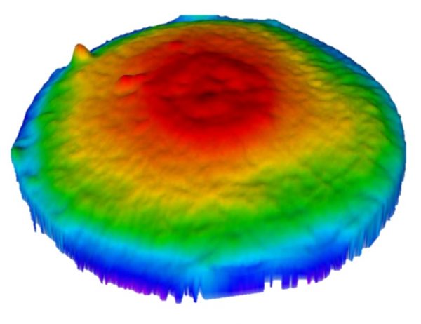
3D Wafer Flatness Measurement
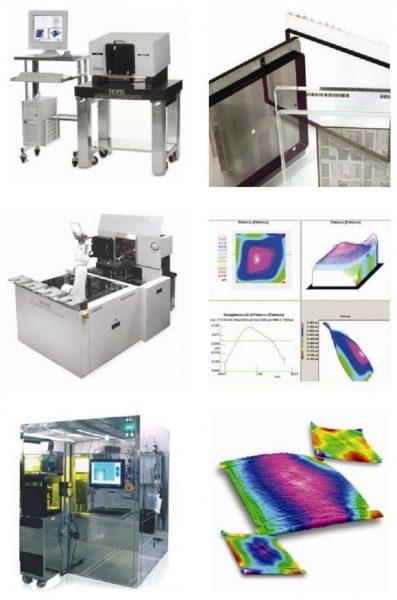
Corning Tropel® Metrology Instruments
Tropel Metrology Instruments creates measurement solutions for a variety of challenging industrial problems revolving around the manufacture of precision flat surfaces.
- Fast – Full surface measurements in seconds
- Powerful – Highly customizable analysis, without the operators‘ influence
- Accurate – Sub-micron accuracy and repeatability
- Easy to Use – Load the part and press measure

Do You Have Questions?
Feel free to give us a call:
+49 89 35 09 578 -0
Klaus Gailus
Tropel® Metrology Instruments offer contactless full surface analysis tools for QC labs as well as for high volume productions. The laser interferometers like the Tropel® FlatMaster®, the Tropel® UltraSort, and the Tropel® UltraFlat® illuminate and capture entire surfaces at once and thus can measure a variety of surfaces in just a few seconds with sub-micron to nanometer high accuracy. Dimensional measurements can be made to measure surface shapes for flatness, parallelism, height, depth, surface finish, roughness or thickness as well as the typical parameters regarding semiconductor wafers Bow/Warp, global and local flatness along with TTV and thickness.
Those measurement techniques are available in manual, semi-manual or fully automatic handlings.
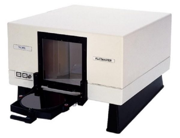
FlatMaster FM200Wafer
Corning Tropel® FlatMaster®
The Tropel® FlatMaster® offers surface form measurements through a laser interferometer based on grazing incidence interferometry. It provides five-nanometers resolution with a standard accuracy of 50nm (2.0 μ”). The non-contact optical technique used in the process analyzes the entire surface in seconds and accurately measures flatness, line profile, radius, and other surface parameters on a variety of materials and surface finishes, regardless of its size or complexity.
To optimize the accuracy of the measurements the Tropel® FlatMaster® is available in several standard versions to rapidly and accurately measure different component size ranges. The FlatMaster® 40, 100, and 200 measures parts up to 40 mm, 100 mm, and 200 mm respectively and it measures larger parts by stitching multiple measured segments together.
To achieve specific performance requirements and conditions a custom-made option is available as well to compose an instrument fitted for different increasing dynamic ranges, accuracy, or to include component handling features.
Download data sheet:
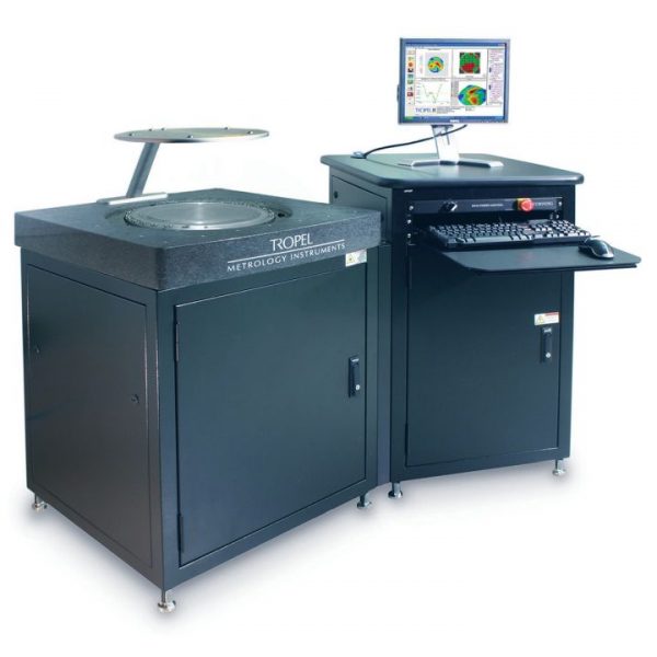
FlatMaster MSP300
Corning Tropel® FlatMaster® MSP
To successfully integrate 3DIC assemblies it is critical to measure the thickness, roughness, and flatness variations of glass and wafers up to 300 millimeters; conventional optical probes or interferometric systems are too slow or do not have the required accuracy or measurement ranges.
The Tropel® FlatMaster® MSP (Multi-Surface Profiler) is a non-contact frequency scanning interferometer that measures multiple surfaces simultaneously. It offers an accurate and fast optical metrology for semiconductor wafers with diameters up to 300 millimeters. That way the FlatMaster is the first instrument that collects and analyzes up to 3 million data points in just a few seconds, providing a thickness, parallelism, height/depth, and flatness characterization of the entire surface. In a different configuration, the MSP could be configured to measure surface roughness as well.
The FlatMaster MSP offers robust metrology for a wide range of applications, ranging from complex components, assemblies to transparent materials, and wafer metrology. Furthermore, in the dual-head configuration, the parallelism of opposite surfaces and the thickness can be absolutely determined. The FlatMaster MSP-DH is the dual-head option and configured to measure two sides of a component or an assembly to provide the absolute thickness and parallelism measurements.
Download data sheet:
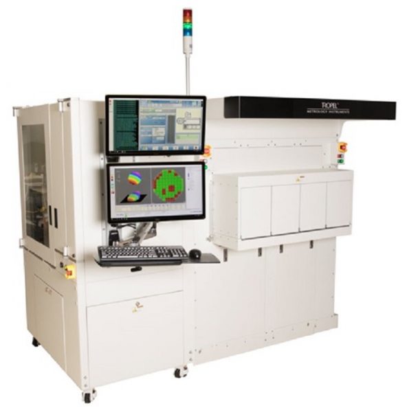
UltraSort II, Automatic Wafer Metrology System
Corning Tropel® UltraSort®
The Tropel® UltraSortTM was designed for volume wafer production and offers automated system superior performance in the rapid, repeatable, accurate, non-contact qualification of silicon and alternative substrate wafers.
UltraSort is an automatic wafer flatness analysis system that includes cassette-to-cassette wafer handling with user-configurable sorting capability and provides an in-depth photomask inspection. This Class 100 cleanroom compliant system combines a grazing-incidence interferometer with industry-standard robotic handling. The UltraSort can be configured to measure wafer sizes from 2 inches to 8 inches in diameter and is well suited for a variety of different materials including gallium arsenide, sapphire, quartz, germanium, silicon, silicon carbide, and many others.
The UltraSort II is a flexible, high-throughput, fully automated platform that incorporates any Tropel wafer flatness measurement system, providing full surface bow, warp, TTV, and stepper simulation parameters as described in SEMI M1. The UltraSort II can also accept modules including extra cassettes, another interferometer, OCR, ROA, and many more. That system allows us to get more out of the automated optical wafer flatness and roughness inspection system and comes with a wafer OCR. The UltraSort II platform is designed to enable full factory automation including SECS/GEM, GEM 300 host systems, along with other custom data export systems.
Download data sheet:
UltraFlat, General Systems
Corning Tropel® UltraFlat®
Corning Announces Tropel® UltraFlat™ for EUV System
The Tropel® UltraFlat System was specifically designed for the photomask industry; it is a new photomask measurement system created to help semiconductor manufacturers meet the ever-tightening mask flatness specifications for extreme ultraviolet (EUV) semiconductor lithography. Due to the new flatness requirements, it delivers the lowest measurement uncertainty possible. As a consequence of the shrinking features, not only flutter wafers are required, but flutter masks as well. The UltraFlat system measures photo-blanks and photomasks consistently in every step of production and performance, which includes substrate polishing, coating, and patterning to analyze film stress, and verification. The UltraFlat system employs near-normal incidence interferometry, rock-solid structural design, state-of-the-art optical fabrication techniques, and Tropel’s renowned phase-shifting analysis software to achieve six-nanometers uncertainty. It provides NIST traceability and conforms to the SEMI standard measurements. Also available are additional automated photomask handling, measurement configurations, and clean room options.
Download data sheet:
Conference Presentation:
With almost 170-years of expert know-how, Corning is one of the leading innovators in glass science, ceramic science, and optical physics. The expertise in the latter as well as in specialty glass results in diversified products such as full optical systems, including automated laser glass-cutting and non-contact metrology instruments; These products are served especially on the display, automobile, and semiconductor markets.

Tropel ® Metrology Instruments, a subsidiary of Corning Incorporated located in Fairport, NY, USA is one of the world’s leading companies in non-contact optical metrology for high precision components for the semiconductor and mechanical industries.
Do You Have Questions?
Feel free to give us a call:
+49 89 35 09 578 -0
Klaus Gailus

Do You Have Questions?
Feel free to give us a call:
+33 476 350 707
Pascal Gautraud